
High-Purity Gold (Au1)
Purity ≥99.999%, available in flake and cylinder forms. Custom specifications supported.

Semiconductor Packaging Materials
Material selection catalog covering deposition materials, sputtering targets, bonding wires, preformed solder wafers, and SMT materials—from wafer fabrication to packaging and testing. Small-batch ordering available with full batch traceability; grades matched to specific process steps.
≥99.999%
Deposition Material Purity
10+
Sputtering Target Grade
50+
Pre-formed solder alloy
φ10μm
Smallest Bonding Wire Diameter
Organize the material catalog by key processes such as wafer fabrication, packaging and interconnection, and surface mount technology to reduce selection trial-and-error.
Incoming and outgoing materials undergo purity, wire diameter, and alloy system testing with retained samples; batch information is fully traceable.
Supports sample and low-volume orders to reduce validation costs during new material onboarding.
Provide process details for same-day feedback on available materials and specification recommendations.
BY PROCESS · Materials Line
From wafer fabrication to packaging and testing, organize materials by process step to help procurement and engineering teams quickly locate grades and specifications.
Purity ≥99.999%, available in flake and cylinder forms. Custom specifications supported.

Purity ≥99.999%, with extremely low C, N, and O impurities; features low and stable contact resistance, easy film formation, excellent fusion capability, and strong adhesion to the semiconductor substrate.

Purity ≥ 99.999%
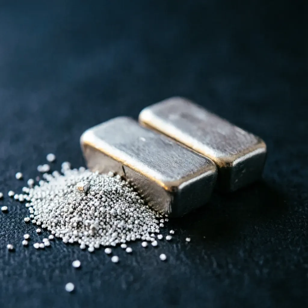
Purity ≥ 99.99%
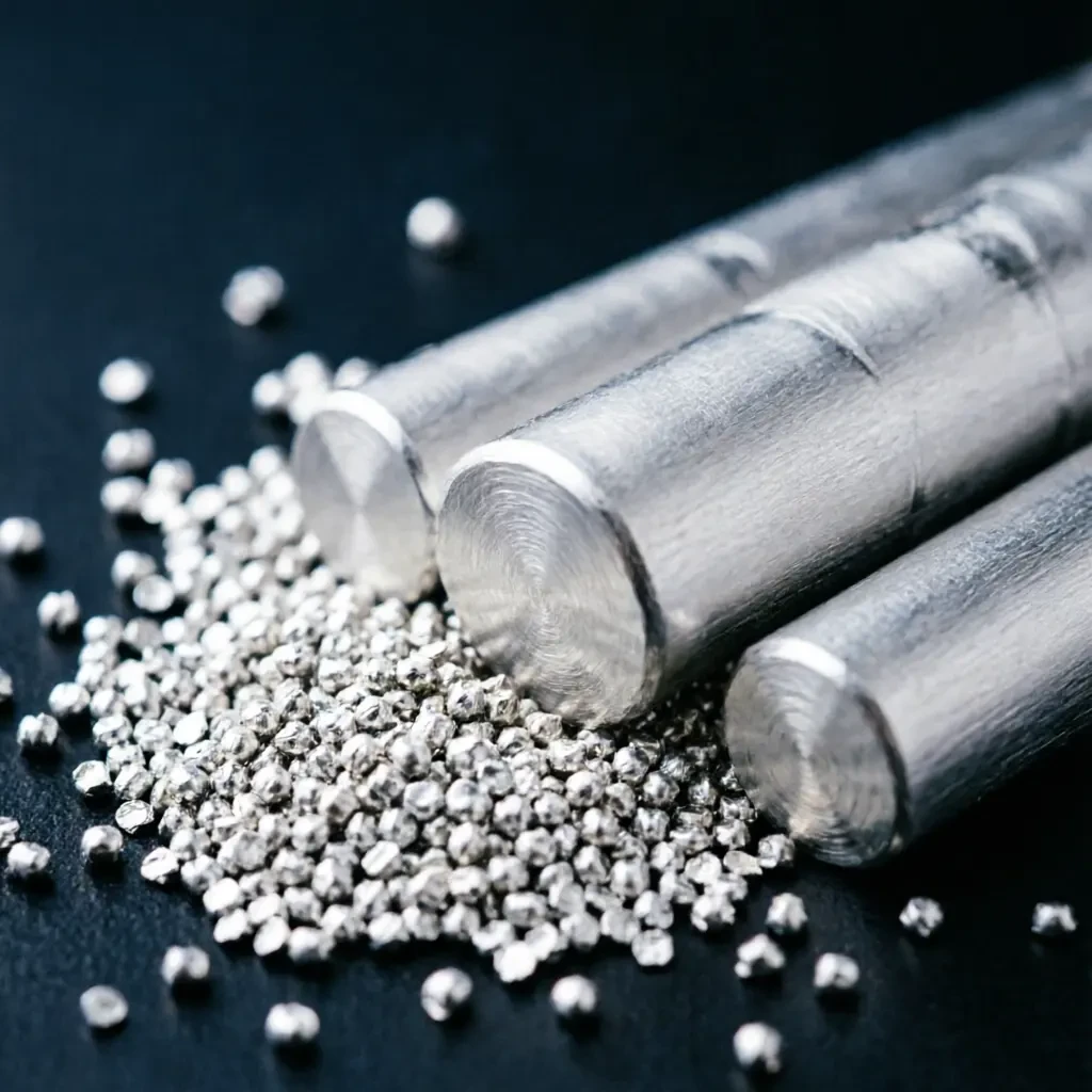
Purity options: 4N / 5N / 5N5

Purity options: 4N / 4N5 / 5N
INSIGHTS · News & Updates
Company news, product launches, and selection guides—browse by category to find what matters most.

Adds custom shapes such as square and U-shaped to the standard rectangular, washer, and disc formats. Supports flux coating, tape-and-reel packaging, and glass bottle packaging.

Re-test the purity of high-purity silver Ag01 batches and retain samples. Test data will be provided with batch shipments to facilitate customer traceability for batch consistency.

Bonding wire G2 / GK / GJ covers a diameter range of φ10~80μm. Select the appropriate specification based on package type and reliability grade.
INDUSTRY APPLICATIONS
Demonstrate how our materials solve real-world problems in your manufacturing processes. We break down each solution by addressing pain points, recommending the optimal material, and detailing key performance parameters.

ABOUT GETAITECH
Shenzhen Getai Technology Co., Ltd. specializes in supplying materials and technical support for semiconductor packaging and electronic assembly. Our product portfolio includes evaporation materials, sputtering targets, bonding wires, preforms, and SMT materials, serving industries such as semiconductor packaging, wafer testing, photovoltaics, flat panel displays, and precision electroplating. We organize our material catalog by process step to help procurement and engineering teams quickly map process requirements to specific grades and specifications.
INQUIRY
Submit process steps, packaging format, and key parameter requirements. We will provide feedback on available materials and specifications the same day, supporting sample and small-batch validation.


